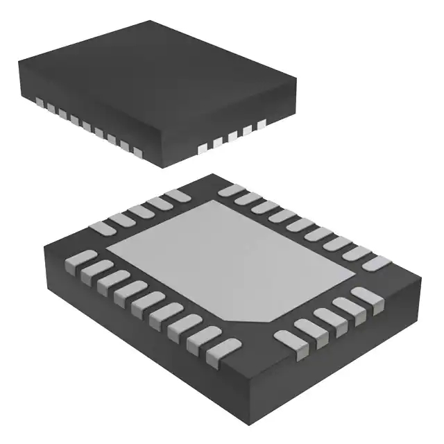
In the world of electronics manufacturing, surface mount package sizes play a crucial role in determining the form, functionality, and performance of integrated circuits. These package sizes, often referred to as form factors, have a significant impact on the overall design and functionality of electronic devices. In this article, we will explore the various surface mount package sizes commonly used in the industry, their importance, and factors to consider when selecting the right package size for your application.
1. Introduction
In the realm of electronic components, surface mount technology (SMT) has revolutionized the way circuits are assembled and manufactured. Unlike through-hole mounting, where components are inserted into pre-drilled holes on a circuit board, surface mount technology allows for the direct placement of components on the surface of the board. This method offers several advantages, including increased component density, smaller board sizes, and improved manufacturing efficiency.
2. What are Surface Mount Package Sizes?
Surface mount package sizes refer to the physical dimensions and configurations of integrated circuit packages used in surface mount technology. These packages are designed to house electronic components such as microchips, transistors, and diodes, and facilitate their soldering onto the circuit board. The package size determines the space required for mounting the component and influences the electrical and thermal characteristics of the device.
3. Importance of Surface Mount Package Sizes
Choosing the appropriate surface mount package size is vital for the successful integration of components into a circuit design. The size of the package affects various aspects of the electronic device, including its overall size, power consumption, heat dissipation, and signal integrity. Therefore, understanding the importance of surface mount package sizes is crucial for electronic engineers and designers.

4. Common Surface Mount Package Sizes
There are numerous surface mount package sizes available in the market, each with its own advantages and applications. Here are some of the most commonly used surface mount package sizes:
4.1 Small Outline Integrated Circuit (SOIC)
The Small Outline Integrated Circuit (SOIC) package is a popular choice for many electronic devices. It features a small form factor, typically rectangular in shape, with leads extending from two sides of the package. SOIC packages are available in various pin counts, making them versatile for different applications.
The Quad Flat Package (QFP) is another widely used surface mount package size. It features a square or rectangular body with leads extending from all four sides of the package. QFP packages offer high pin density, making them suitable for complex integrated circuits that require numerous input and output connections.
The Ball Grid Array (BGA) package has gained popularity due to its excellent thermal and electrical performance. BGA packages consist of a substrate with an array of solder balls on the bottom side, which enables direct mounting onto the circuit board. They are commonly used in high-performance applications such as microprocessors and graphics chips.
The Dual In-Line Package (DIP) is one of the oldest and most recognizable package sizes. DIP packages feature two parallel rows of leads extending from opposite sides of the package. They are commonly used for through-hole mounting but also have surface mount variants available. DIP packages are often used for discrete components and integrated circuits with lower pin counts.

The Thin Small Outline Package (TSOP) is a surface mount package size that is frequently used in memory chips, such as flash memory and dynamic random-access memory (DRAM). TSOP packages have a thin body with leads extending from two sides, allowing for compact designs and efficient use of board space.
4.6 Small Outline Transistor (SOT)
The Small Outline Transistor (SOT) package is primarily used for discrete transistors and other small-scale components. SOT packages are available in various sizes and pin configurations, making them suitable for a wide range of applications. They are often used in consumer electronics, automotive systems, and telecommunications devices.
5. Factors Affecting Surface Mount Package Sizes
When selecting a surface mount package size, several factors need to be considered. These factors will influence the performance, reliability, and overall functionality of the electronic device. Here are some key factors that affect surface mount package sizes:
5.1 Pin Count
The number of pins required for the integrated circuit or component is a crucial consideration. Higher pin counts may necessitate larger package sizes to accommodate the required connections. It is essential to assess the pin count requirements based on the functionality and complexity of the circuit.
5.2 Functionality
The intended functionality of the electronic device plays a significant role in determining the appropriate package size. Certain applications may require specific package sizes to meet performance criteria, such as high-frequency operation, low power consumption, or thermal dissipation.
5.3 Thermal Considerations
Heat dissipation is a critical aspect of electronic device design. Some components generate more heat than others, and the package size can affect the ability to dissipate that heat effectively. Larger package sizes often offer better thermal characteristics, allowing for improved heat transfer and dissipation.
6. Selecting the Right Surface Mount Package Size
Choosing the right surface mount package size involves evaluating multiple factors to ensure optimal performance and reliability. Here are some considerations when selecting a package size for your application:
6.1 Application Requirements
Understanding the specific requirements of your application is crucial. Determine the necessary pin count, thermal considerations, and electrical characteristics needed to meet the desired functionality and performance.
6.2 Board Space Constraints
Consider the available board space and size limitations. Smaller package sizes are often preferred when space is limited, but be cautious of potential signal integrity issues or thermal constraints that may arise due to compact designs.
6.3 Manufacturing Considerations
The chosen package size should align with your manufacturing capabilities and processes. Some package sizes may be more challenging to assemble or may require specialized equipment, which can impact the overall cost and feasibility of production.

7. Industry Trends in Surface Mount Package Sizes
The field of surface mount technology is constantly evolving, driven by advancements in semiconductor manufacturing and the demand for smaller, more powerful electronic devices. Industry trends include the development of smaller package sizes with increased pin densities, improved thermal management techniques, and the integration of multiple functions within a single package.
8. Conclusion
Surface mount package sizes play a vital role in electronic device design and manufacturing. Selecting the appropriate package size is crucial for achieving the desired functionality, performance, and reliability. By considering factors such as pin count, functionality, and thermal considerations, designers can make informed decisions and optimize their circuit designs for the intended application.
9. FAQs
Q1. Are surface mount package sizes standardized?
Surface mount package sizes are not standardized across all manufacturers. While there are industry-standard package sizes available, some manufacturers may offer proprietary packages with unique form factors.
Q2. Can I interchange different surface mount package sizes for the same component?
Interchanging surface mount package sizes for the same component is generally not recommended. Each package size has specific electrical and thermal characteristics that may affect the overall performance of the component.
Q3. How do I determine the pin count for a specific component?
The pin count for a component is typically specified in its datasheet. Refer to the manufacturer's documentation or contact our technical support for accurate pin count information.
Q4. Are smaller package sizes always better?
Smaller package sizes are advantageous when board space is limited. However, it is essential to consider other factors such as thermal management and signal integrity to ensure the optimal performance of the component.
Q5. What are some emerging surface mount package technologies to watch out for?
Emerging technologies in surface mount packages include wafer-level chip-scale packages (WLCSP), package-on-package (PoP), and system-in-package (SiP). These technologies offer compact designs, increased functionality, and improved performance for advanced electronic applications.


Comments
0